49D61239-D69F-426A-86DF-819E74BB0CEB
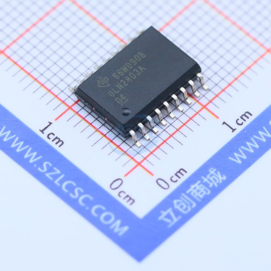
ULN2803ADWR
50-V, eight-channel darlington array
現有庫存 10,000NT$ 35/ 件
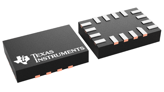
Four-bit dual-supply bus transceiver with configurable voltage-level shifting and tri-state outputs
現有庫存 51,000加入清單後可統一送出詢價。送出詢價不會扣款或保留庫存。
需要協助選型?聊聊這項產品 ↗Four-bit dual-supply bus transceiver with configurable voltage-level shifting and tri-state outputs
Each channel has an independent DIR control input Control inputs VIH/VIL levels are referenced to VCCA voltage Fully configurable dual-rail design allows each port to operate over the full 1.1V to 3.6V power-supply range I/Os are 4.6V tolerant Ioff Supports partial power-down-mode operation Typical data rates 380Mbps (1.8V to 3.3V translation) 200Mbps (<1.8V to 3.3V translation) 200Mbps (translate to 2.5V or 1.8V) 150Mbps (translate to 1.5V) 100Mbps (translate to 1.2V) Latch-up performance exceeds 100 mA Per JESD 78, class II ESD Protection exceeds the following levels (tested per JESD 22) ±8000V Human-body model (A114-A) 250V Machine model (A115-A) ±1500V Charged-device model (C101)
This 4-bit noninverting bus transceiver uses two separate configurable power-supply rails. The A port is designed to track VCCA. VCCA accepts any supply voltage from 1.1 V to 3.6V. The B port is designed to track VCCB. VCCB accepts any supply voltage from 1.1 to 3.6V. The SN74AVC4T774 is optimized to operate with VCCA/VCCB set at 1.4V to 3.6V. It is operational with VCCA/VCCB as low as 1.2V. This allows for universal low-voltage bi-directional translation between any of the 1.2V, 1.5V, 1.8V, 2.5V, and 3.3V voltage nodes. The SN74AVC4T774 is designed for asynchronous communication between data buses. The logic levels of the direction-control (DIR) input and the output-enable ( OE) input activate either the B-port outputs or the A-port outputs or place both output ports in the high-impedance mode. The device transmits data from the A bus to the B bus when the B outputs are activated, and from the B bus to the A bus when the A outputs are activated. The input circuitry on both A and B ports is always active and must have a logic HIGH or LOW level applied to prevent excess ICC and ICCZ. The SN74AVC4T774 is designed so that the control pins (DIR1, DIR2, DIR3, DIR4, and OE) are supplied by VCCA. This device is fully specified for partial-power-down applications using Ioff. The Ioff circuitry disables the outputs, preventing damaging current backflow through the device when it is powered down. The VCC isolation feature ensures that if either VCC input is at GND, then both ports are in the high-impedance state. For a high-impedance state during power-up or power-down, OE should be tied to VCCA through a pullup resistor; the minimum value of the resistor is determined by the current-sinking capability of the driver. Since this device has CMOS inputs, it is very important to not allow them to float. If the inputs are not driven to either a high VCC state, or a low-GND state, an undesirable larger than expected ICC current may result. Since the input voltage settlement is governed by many factors (for example, capacitance, board-layout, package inductance, surrounding conditions, and so forth), ensuring that they these inputs are kept out of erroneous switching states and tying them to either a high or a low level minimizes the leakage-current.
50-V, eight-channel darlington array
現有庫存 10,000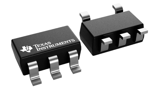
1A loading, 2.7-5.5V, 70mΩ USB power switch, active-high
現有庫存 60,000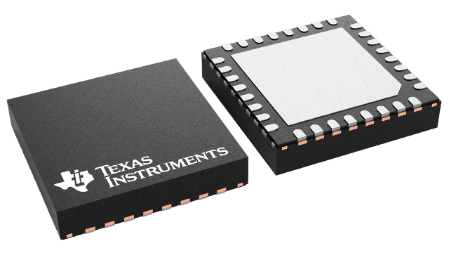
車規級 4.16Gbps 串聯器 (2.3MP/60fps) 4.16Gbps FPD-Link III, MIPI CSI-2, PoC Support, AEC-Q100 Grade 2","ADAS 專用,支援雷達與高解析度攝影機,具備極低延遲控制通道與完整診斷功能。
供貨需確認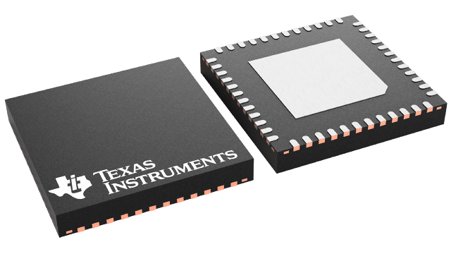
車規級雙通道解串器集線器 (Hub) Dual FPD-Link III Input, MIPI CSI-2 Output, Port Replication, Adaptive EQ","支援雙鏡頭聚合與 2x2 複製模式 (Data Logging),自動補償電纜損耗,適合環視系統。
供貨需確認